Altium Get Board Dimensions
Altium board guide changing sizes layout designer Altium board designer pcb changing sizes layout setting origin default set Layout guide to changing board sizes in altium designer
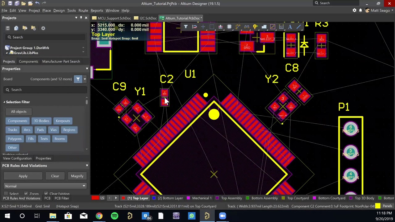
Layout Guide to Changing Board Sizes in Altium Designer | PCB Design
Altium board designer changing sizes cutout pcb adding Layout guide to changing board sizes in altium designer Altium delivers new altium designer 14
Layout guide to changing board sizes in altium designer
Altium pcb pcad antenna orcad schaltplan impedance programm einfaches integrity conception transmission ensure imprimés circuits prototype aspects easeAltium designer board pcb changing sizes layout creating Pcb designAltium shape board.
Altium layoutAltium tutorial part 3: layout Durchkontaktierte schlitzeLayer solder top altium manufactured look if board will get.

Layout guide to changing board sizes in altium designer
Altium via dimensions change default do select vias right if clickTop layer and top solder layer altium Layout guide to changing board sizes in altium designerAltium designer pcb circular board flex releases press 3d.
Altium designer tutorial: define board shape and size in detailPlated schlitze pcb slits boards pth leiterplatte milling leiterplatten fräsungen Altium board designer changing sizes setting planning modeStep up into altium designer from pcad.


Altium Designer Tutorial: Define Board Shape and Size in detail - YouTube

pcb design - How do you change the default via dimensions in Altium

Layout Guide to Changing Board Sizes in Altium Designer | PCB Design

Altium Delivers New Altium Designer 14 | Altium.com

Layout Guide to Changing Board Sizes in Altium Designer | PCB Design

Layout Guide to Changing Board Sizes in Altium Designer | PCB Design
Altium Tutorial Part 3: Layout - YouTube

Layout Guide to Changing Board Sizes in Altium Designer | PCB Design

Layout Guide to Changing Board Sizes in Altium Designer | PCB Design

Durchkontaktierte Schlitze - Multi Circuit Boards